ANASEN: Difference between revisions
Jump to navigation
Jump to search
| Line 1: | Line 1: | ||
= First Generation = | = First Generation = | ||
https://doi.org/10.1016/j.nima.2017.07.030 | NIM paper : https://doi.org/10.1016/j.nima.2017.07.030 | ||
PRC paper : https://doi.org/10.1103/PhysRevC.105.055806 | |||
= Second Generation = | = Second Generation = | ||
Revision as of 17:13, 15 December 2023
First Generation
NIM paper : https://doi.org/10.1016/j.nima.2017.07.030 PRC paper : https://doi.org/10.1103/PhysRevC.105.055806
Second Generation


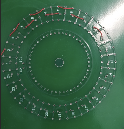
The main difference from the 1st generation is the Twisted Anode and Cathode wires.
Basics Geometry

There are 5 Layers on the radial position of the ANASEN.
| Structure | Radius [mm] |
|---|---|
| ionizing wires | 23 |
| Graurd wires | 33 |
| Anode wires | 38 |
| Cathode wires | 43 |
| SuperX3 Silicon | 88 |
Twisted Anode and Cathodes
Readout
SuperX3 Silicon Detector Array

There are 24 Super-X3 double-sided Silicon detectors on the wall of the ANASEN. They are placed 88 mm away from the beam axis. Each of them has 75 mm X 40 mm sensitive area. Thus, the super-X3 covers a forward and backward angle of 40 deg.