CAEN digitizer: Difference between revisions
(→FSUDAQ) |
|||
| Line 441: | Line 441: | ||
* for Ubuntu 22.04 or equivalent | * for Ubuntu 22.04 or equivalent | ||
The DAQ can be downloaded at https://fsunuc.physics.fsu.edu/git/rtang/FSUDAQ_Qt6 | The DAQ can be downloaded at | ||
*https://fsunuc.physics.fsu.edu/git/rtang/FSUDAQ_Qt6 (development) | |||
*https://github.com/goluckyryan/FSUDAQ (stable, kind of) | |||
== The Digitizer Class == | == The Digitizer Class == | ||
Revision as of 13:28, 13 June 2024
| This page is for the 1st generation digitizer, Here for 2nd generation digitizer. |
Model
| Model | Energy resolution | Sampling rate | No. of Channel |
|---|---|---|---|
| V1725 | 14-bit | 250MS/s = 4 ns | 16 |
| V1730 | 14-bit | 500MS/s = 2 ns | 16 |
| V1740 | 12-bit | 62.5 MS/s = 16 ns | 64 |
DPP firmware
Both V1725 and V1730 can be equipped with the PHA (pulse-height analysis) or PSD (pulse-shape decimation) firmware.
From the programming point of view, the channel registers ( < 0x1XXX ) are very different for the two firmware, but the board registers (0x8000 to 0xFFFF) are almost identical.
required library
On Linux (Ubuntu 18.04+), two CAEN libraries are required to run the digitizers.
- CAENVMELib
- CAENComm
that would be enough for running the CAEN CoMPASS.
For custom programs, an additional library is needed
- CAENDigitizer
PLL (Phase-Locked-Loop) firmware
A digitizer need a proper PLL firmware to run.
If the PLL firmware is wrong (i.e. The PLL lock led is off ), you need to refresh the PLL firmware using the CAENUpgrader
The PLL file has the format of
V17XX_vcxo500_refYY_pll_outZZ.rbf
where
XX is the model type,
for example 25, 25S, 30, 40
YY is the ref clock,
for the master or stand alone digitizer, 50 (= 50 MHz ) is ok.
for a slave, it must be 62_5.
ZZ is the clock output,
for master or stand alone digitizer, 0 or 62_5 (= 62.5) are OK.
for a master that connect to a slave, it must be 62_5.
for a slave, that connect to an other slave, it must be 62_5
PHA Registers
Most of the register settings are trivial and east to understand, here is the list of special registers.
Trapezoid Rescaling
The register 0x1n80 (DPP Algorithm Control) bit [5:0] is the Trapezoid rescaling factor (SHF). It is calculated using the formula
Failed to parse (SVG with PNG fallback (MathML can be enabled via browser plugin): Invalid response ("Math extension cannot connect to Restbase.") from server "https://wikimedia.org/api/rest_v1/":): {\displaystyle \textrm{SHF} = \lfloor \log_2( k * M) \rfloor }
Failed to parse (SVG with PNG fallback (MathML can be enabled via browser plugin): Invalid response ("Math extension cannot connect to Restbase.") from server "https://wikimedia.org/api/rest_v1/":): {\displaystyle k = } trapezoid rise time in the register
Failed to parse (SVG with PNG fallback (MathML can be enabled via browser plugin): Invalid response ("Math extension cannot connect to Restbase.") from server "https://wikimedia.org/api/rest_v1/":): {\displaystyle M = } input decay time in the register
For example, if the rise time is 4000 ns ( = 250), decay time is 50 us ( = 3125 ), then then SHF = . This is the standard scaling, meaning the internal trapezoid waveform (48 bits) is right-bit-shifted by 19 (i.e. >> 19 ) to a 15-bit value.

fine gain 0x1nC4
fine gain = Failed to parse (SVG with PNG fallback (MathML can be enabled via browser plugin): Invalid response ("Math extension cannot connect to Restbase.") from server "https://wikimedia.org/api/rest_v1/":): {\displaystyle f } is a 16-bit value (0 - 65535 = 0xFFFF ) calculated by
Failed to parse (SVG with PNG fallback (MathML can be enabled via browser plugin): Invalid response ("Math extension cannot connect to Restbase.") from server "https://wikimedia.org/api/rest_v1/":): {\displaystyle f = \textrm{0xFFFF} \times \frac{2^{\textrm{SHF}}}{k M} \times \alpha }
Failed to parse (SVG with PNG fallback (MathML can be enabled via browser plugin): Invalid response ("Math extension cannot connect to Restbase.") from server "https://wikimedia.org/api/rest_v1/":): {\displaystyle \alpha = } the desired physical fine gate, range 0 to Failed to parse (SVG with PNG fallback (MathML can be enabled via browser plugin): Invalid response ("Math extension cannot connect to Restbase.") from server "https://wikimedia.org/api/rest_v1/":): {\displaystyle k M / 2^{\textrm{SHF}} }
For example, the rise time and decay are the same as above, Failed to parse (SVG with PNG fallback (MathML can be enabled via browser plugin): Invalid response ("Math extension cannot connect to Restbase.") from server "https://wikimedia.org/api/rest_v1/":): {\displaystyle 2^{\textrm{SHF}} / k / M = 0.671 } , so that the maximum desired fine gate Failed to parse (SVG with PNG fallback (MathML can be enabled via browser plugin): Invalid response ("Math extension cannot connect to Restbase.") from server "https://wikimedia.org/api/rest_v1/":): {\displaystyle \alpha = 1.49 }
The FSUDAQ always set Failed to parse (SVG with PNG fallback (MathML can be enabled via browser plugin): Invalid response ("Math extension cannot connect to Restbase.") from server "https://wikimedia.org/api/rest_v1/":): {\displaystyle \alpha = 1 }
DC offset 0x1n98
This is a 16-bit register. The percentage DC offset Failed to parse (SVG with PNG fallback (MathML can be enabled via browser plugin): Invalid response ("Math extension cannot connect to Restbase.") from server "https://wikimedia.org/api/rest_v1/":): {\displaystyle \beta } to register value is Failed to parse (SVG with PNG fallback (MathML can be enabled via browser plugin): Invalid response ("Math extension cannot connect to Restbase.") from server "https://wikimedia.org/api/rest_v1/":): {\displaystyle \textrm{0xFFFF} \times ( 1 - \beta ) }
For example, a 40% DC offset, the register value is Failed to parse (SVG with PNG fallback (MathML can be enabled via browser plugin): Invalid response ("Math extension cannot connect to Restbase.") from server "https://wikimedia.org/api/rest_v1/":): {\displaystyle \textrm{0xFFFF} \times 0.6 = 0x9999 }
Synchronization of multiple digitizers
This is important when multiple digitizers are used. A digitizer using its internal clock (controlled by a switch on the board) is a designated Master. Synchronization means:
- Same source of clock
- Same phase (or constant difference in phase, it can be corrected by the Run delay (0x8170))
- Same starting time for ACQ
Notice that a Timer Reset can be done by writing the Software Clear register (0xEF28), but it does not guarantee all timers are clear at the same time. The Software clear is done whenever ACQ starts.
Master and Slaves Method
The CLK-out of the Master connects to the CLK-in of the slave in the daisy chain. And all slaves should use an external clock. The PLL firmware must be changed properly in order for the clocks of the master and the slaves to be locked and sync.
External Clock unit, everyone is slave Method
testing clocks
The TRG-OUT can be set with register 0x811C to be CLKOUT or CLK Phase. so that the synchronization can be checked.
TRG-IN/TRG-OUT daisy chain
Connect the TRG-IN (Master) to TRG-OUT (Slave). All slaves are set the ACQ start/stop on the TRG-IN (0x8100:[1:0]). The Master is set the ACQ star/stop to SW trigger, and the TRI-OUT is RUN (0x811C::[19:16]).
Once the master ACQ is started by SW, its TRG-OUT will send RUN signal and propagate to the slave TRG-IN that the slaves will be start/stop accordingly.
using S-IN with external TTL/NIM pulse
All master and slaves are set the ACQ start/stop to be S-IN, and TRG-OUT are S-IN (copy of S-IN). Master and slaves are connected TRG-OUT/S-IN daisy chain.
An external gate generator is needed to send an ACQ start signal to the master S-IN to start the data acquisition.
Triggering
Below is the Trigger Logic, the register is for DPP-PHA firmware.

Channel or Coupled Channel
| PHA | PSD | QDC | Bit | Description |
|---|---|---|---|---|
| 0x1n80 | 0x1n80 | 0x1n40 | 19:18 | DPP Algorithm Control, Trigger Mode. |
| 24 | DPP Algorithm Control, Disable self trigger | |||
| 0x1n84 | 0x1n70 | 0x1n78 | PHA/PSD : Shaped Trigger Width QDC : Trigger Out Width | |
| 0x1nA0 | 0x1084 | N/A | 2:0 | DPP Algorithm Control 2, Local Shaped Trigger Mode |
| 6:4 | DPP Algorithm Control 2, Local Trigger Validation Mode | |||
| 15:14 | DPP Algorithm Control 2, Source of veto | |||
| 0x1nDA | 0x1nD4 | N/A | Veto Width | |
| 0x8180 + 4n | 0x810 + 4n | N/A | Trigger Validation Mask | |
| N/A | 0x106C | N/A | Trigger Latency |
Board
| Register | ! Bit | Description |
|---|---|---|
| 0x810C | Global Trigger Mask or Logic | |
| 0x8110 | Front Panel TRG-OUT Logic | |
| 0x811C | 10 | TRG-IN control |
| 11 | TRG-IN to Mezzanines (Channel FPGA) |
Single board
Scenario 0
No coincident, or self trigger.
0x1n80 0x00000 0xC0000 // set Trigger mode to Normal mode or Independent mode at DPP Algorithm Control.
Scenario 1
Ch-1 is triggered from Ch-0, no matter there si signal for Ch-0
0x1080  0x40000 0xC0000 // Ch-0 to be Coincident
0x10A0  0x70 0xF0  // The local Trigger validation is OR. i.e. from any channel.
0x10A0  0x5  0xF // The local Shaped Trigger for Coupled channel-0 is from the even channel (i.e. ch-0)
Scenario 2
Coincident of ch-0 and ch-1 when both channels are within 1000 ns or 125 ticks.
Register Setting for DPP-PHA is:
0x1084  0x7D             // set the shaped trigger width is 1000 ns for channel 0
0x1184  0x7D             // set the shaped trigger width is 1000 ns for channel 1
0x1080  0x40000  0xC0000 // set channel-0 to be coindient mode
0x1180  0x40000  0xC0000 // set channel-0 to be coindient mode
0x10A0  0x00     0x7     // Enable local Shaped Trigger, AND mode
Scenario 3
when ch-0 is fired and triggered, if ch-7 is also fired, record both ch-0 and ch-7. When ch-0 is fired and triggered, but if ch-7 has nothing, don't need to record ch-7 but only ch-0.
Register Setting for DPP-PHA in the free writefile:
//boardID address value mask
0-14-177 0x10A0 0x5     0x7      //DPP Algorithm Control 2 for channel-0, bit[2:0] = 101. Enable local Shaped Trigger, Mode is even channel of the coupled channel ONLY.
0-14-177 0x1780 0x40000 0xC0000  //DPP Algorithm Control for channel-7, bit[19:18] = 01. Trigger mode = Coincidence Mode
0-14-177 0x1784 0xFF    0x3FF    //Shaped Trigger Width for channel-7, bit[9:0] = 00 1111 1111. Generate Shaped trigger of 255 * 16 ns.
0-14-177 0x16A0 0x50    0x70     //DPP Algorithm Control 2 for channel-6, bit[6:4] = 101. Enable local Trigger Validation, Mode is val0 = val1 = signal from mother board mask.
0-14-177 0x818C 0x1     0xFF     //Trigger Validation Mask for the 3rd (4*3 = C) coupled channels (ch-6-7). bit[7:0] =  0000 0001. Set trigger of coupled channel 3 from coupled channel 0.
In FSUDAQ, in the Digitizer Settings Panel,
- Set the ch-0, Local Shaped trig. [G] to be The even Channel


- Set the ch-7, Trig Mode to be Coincident, Local Trig. Valid. [G] to be Equal
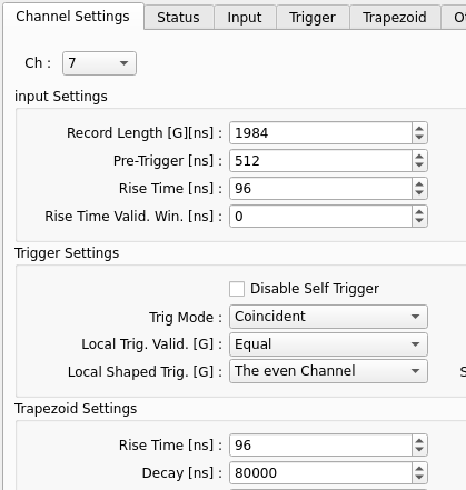

- In the board setting, go to the Trigger Mask tap, and set row 6-7, column 0-1.


Notice that the ch-6 will be triggred. To avoid this, can disable ch-6, or set ch-6 Trig. Mode to be Coincident.
Multiple boards
The idea is very similar to the case of a single board. The only differences are in using TRG-IN and TRG-OUT. The Individual Trigger (ITRG) is included in the TRG-IN, we can send a TRG-OUT signal (controlled by 0x8110) to the TRG-IN of the other boards for the trigger.
Reading the bin file from CAEN CoMPASS
The CoMPASS can output *.bin data. The beginning of the file is a 2 bytes header. It must be in the form of 0xCAEx, where x indicate the energy format and waveform existence.
| last 4 bit of the header | meaning |
|---|---|
| b0001 | Energy in Channel, 16 bit |
| b0010 | Energy in MeV or KeV, 64 bit double |
| b0011 | Energy in Channel (16-bit) + Energy in MeV or KeV (64 bit double) |
| b0100 | Energy is Channel, 16 bit |
| b1000 | Waveform is recorded |
If x < 8, there is no waveform.
After that,
| block | bytes |
|---|---|
| Board | 2 |
| Channel | 2 |
| Timestamp | 8 |
| Energy | [x == 1, 2], [x == 2, 8], [x == 3, 10], [x == 4, 2] |
| Flags | 4 |
| Waveform code | 1 |
| number of samples | 4 |
| trace ... | 2 * (number of samples) |
A BinReader class can be found in here.
Data structure, Read-out, and buffer size
The data and the readout are controlled by the following registers
| Register PHA or PSD | Register QDC | Symbol | Max | Name | Function |
|---|---|---|---|---|---|
| 0x800C | 0x800C | Failed to parse (SVG with PNG fallback (MathML can be enabled via browser plugin): Invalid response ("Math extension cannot connect to Restbase.") from server "https://wikimedia.org/api/rest_v1/":): {\displaystyle N_b} | 0xA | Agg. Organization | divide the memory of a channel by Failed to parse (SVG with PNG fallback (MathML can be enabled via browser plugin): Invalid response ("Math extension cannot connect to Restbase.") from server "https://wikimedia.org/api/rest_v1/":): {\displaystyle 2^{N_b}} parts |
| 0x1n34 | 0x8020 | Failed to parse (SVG with PNG fallback (MathML can be enabled via browser plugin): Invalid response ("Math extension cannot connect to Restbase.") from server "https://wikimedia.org/api/rest_v1/":): {\displaystyle N_e} | 511 | Event/Agg | number of event in a agg. and the number of event in a memory division |
| 0xEF1C | 0xEF1C | Failed to parse (SVG with PNG fallback (MathML can be enabled via browser plugin): Invalid response ("Math extension cannot connect to Restbase.") from server "https://wikimedia.org/api/rest_v1/":): {\displaystyle N_a} | 1023 | Max Agg/Read | max number of Agg. pre readout call |
| 0x1n20 | 0x8024* | Failed to parse (SVG with PNG fallback (MathML can be enabled via browser plugin): Invalid response ("Math extension cannot connect to Restbase.") from server "https://wikimedia.org/api/rest_v1/":): {\displaystyle N_s} | 12 bit | Record Length | in QDC, the register 0x8024 is only for write, reading use register 0x1024. |
| 0x8000 | 0x8000 | Failed to parse (SVG with PNG fallback (MathML can be enabled via browser plugin): Invalid response ("Math extension cannot connect to Restbase.") from server "https://wikimedia.org/api/rest_v1/":): {\displaystyle E_x} | 1 bit | DPP Algorithm (bit 17) | Enable Extra |
In the CAENDigitizer.h, the CAEN_DGTZ_READDATA() will read the buffer of the digitizer. For a single call of the function, Failed to parse (SVG with PNG fallback (MathML can be enabled via browser plugin): Invalid response ("Math extension cannot connect to Restbase.") from server "https://wikimedia.org/api/rest_v1/":): {\displaystyle N_a} block aggregate of data is read from the buffer and clear. The data structure started with 4 words header( 1 word = 32 bits). It follows with dual (or group) channel aggregate. In PHA or PSD firmware, up to 8? channel aggregates in a block aggregate. In each channel aggregate, it must have Failed to parse (SVG with PNG fallback (MathML can be enabled via browser plugin): Invalid response ("Math extension cannot connect to Restbase.") from server "https://wikimedia.org/api/rest_v1/":): {\displaystyle N_e} events. The digitizer buffer ONLY be ready for ready out when Failed to parse (SVG with PNG fallback (MathML can be enabled via browser plugin): Invalid response ("Math extension cannot connect to Restbase.") from server "https://wikimedia.org/api/rest_v1/":): {\displaystyle N_e} events in one memory division. When Failed to parse (SVG with PNG fallback (MathML can be enabled via browser plugin): Invalid response ("Math extension cannot connect to Restbase.") from server "https://wikimedia.org/api/rest_v1/":): {\displaystyle N_e} set to zero, the digitizer (mysteriously) auto-set the value.
General Idea on the Settings
For low input trigger rate, set the Failed to parse (SVG with PNG fallback (MathML can be enabled via browser plugin): Invalid response ("Math extension cannot connect to Restbase.") from server "https://wikimedia.org/api/rest_v1/":): {\displaystyle N_e} to be small, so the data can be ready for read out fast. While the Failed to parse (SVG with PNG fallback (MathML can be enabled via browser plugin): Invalid response ("Math extension cannot connect to Restbase.") from server "https://wikimedia.org/api/rest_v1/":): {\displaystyle N_e} is small, set the Failed to parse (SVG with PNG fallback (MathML can be enabled via browser plugin): Invalid response ("Math extension cannot connect to Restbase.") from server "https://wikimedia.org/api/rest_v1/":): {\displaystyle N_b} large so that most of the memory is being used and reduce the death time.
The only caution is Failed to parse (SVG with PNG fallback (MathML can be enabled via browser plugin): Invalid response ("Math extension cannot connect to Restbase.") from server "https://wikimedia.org/api/rest_v1/":): {\displaystyle N_b} should not set too large, so that the memory of each division is small. See the Memory Overflow.
It is almost no harm to set Failed to parse (SVG with PNG fallback (MathML can be enabled via browser plugin): Invalid response ("Math extension cannot connect to Restbase.") from server "https://wikimedia.org/api/rest_v1/":): {\displaystyle N_a} to be high, as this is the maximum number of block to be read.
Group (or Dual) Channel Block

The number of hits for a Dual-channel block is controlled by the register 0x1n34 for PHA. The block can only be read when the block is fully filled except for forced flushing via register 0x1n3C (write-only). For example, if Failed to parse (SVG with PNG fallback (MathML can be enabled via browser plugin): Invalid response ("Math extension cannot connect to Restbase.") from server "https://wikimedia.org/api/rest_v1/":): {\displaystyle N_e = 100} , when the trigger rate is only 10 Hz, a dual-channel block can be read every 10 sec.
In x725 or x730 PHA or PSD, channel 2i and 2i+1 are paired or grouped, so it is called Dual Channel Block. In x740, channel 8i to 8i+7 are grouped, so it called Group Channel Block. In general, Channel Block for short.
Each channel Aggregation has 2 words of header. after that is Failed to parse (SVG with PNG fallback (MathML can be enabled via browser plugin): Invalid response ("Math extension cannot connect to Restbase.") from server "https://wikimedia.org/api/rest_v1/":): {\displaystyle N_e} events (0x1n34) for paired channels. In each measurement, there is 1 word of header, Sample/2 words for waveform, 1 word for Extra (if any), and 1 word for Energy, so total = (2 + Sample/2 + Extra), where Sample size is the Record Length = (0x1n20) * 8 ch = Failed to parse (SVG with PNG fallback (MathML can be enabled via browser plugin): Invalid response ("Math extension cannot connect to Restbase.") from server "https://wikimedia.org/api/rest_v1/":): {\displaystyle 8 N_s} . Extra is controlled by bit[17] of (0x8000), denote as (0x8000:17)
Board Aggregation

The Register 0xEF1C controls the maximum number of Aggregations per read. One aggregation could have many dual-channel blocks. what is the maximum number? 8?
Buffer Size calculation
The data stored in the digitizer can be retrieved using
CAEN_DGTZ_ReadData(int handle, CAEN_DGTZ_ReadMode_t mode, char *buffer, uint32_t *bufferSize);

typedef enum {
  CAEN_DGTZ_SLAVE_TERMINATED_READOUT_MBLT = 0,
  CAEN_DGTZ_SLAVE_TERMINATED_READOUT_2eVME = 1,
  CAEN_DGTZ_SLAVE_TERMINATED_READOUT_2eSST = 2,
  CAEN_DGTZ_POLLING_MBLT = 3,
  CAEN_DGTZ_POLLING_2eVME = 4,
  CAEN_DGTZ_POLLING_2eSST = 5,
} CAEN_DGTZ_ReadMode_t;
The data format of the buffer contains two parts: A whole chuck of the buffer can contain multiple board aggregation (depending on Failed to parse (SVG with PNG fallback (MathML can be enabled via browser plugin): Invalid response ("Math extension cannot connect to Restbase.") from server "https://wikimedia.org/api/rest_v1/":): {\displaystyle N_a} ). Inside a board aggregation, there could be at most 8? Channels Aggregation, depending on the channel mask. Each Channels Aggregation can contain at most Failed to parse (SVG with PNG fallback (MathML can be enabled via browser plugin): Invalid response ("Math extension cannot connect to Restbase.") from server "https://wikimedia.org/api/rest_v1/":): {\displaystyle N_e} measurements.
Each board aggregate has 4 words of header. 1 words = 4 bytes = 32 bits, followed by Failed to parse (SVG with PNG fallback (MathML can be enabled via browser plugin): Invalid response ("Math extension cannot connect to Restbase.") from server "https://wikimedia.org/api/rest_v1/":): {\displaystyle N_a} channel aggregate. Each channel block has Failed to parse (SVG with PNG fallback (MathML can be enabled via browser plugin): Invalid response ("Math extension cannot connect to Restbase.") from server "https://wikimedia.org/api/rest_v1/":): {\displaystyle N_e (2 + E_x + 4N_s)} words.
In Each readout, there can be more than 1 Board Aggregation (0xEF1C). The total buffer size (byte) needed is
Failed to parse (SVG with PNG fallback (MathML can be enabled via browser plugin): Invalid response ("Math extension cannot connect to Restbase.") from server "https://wikimedia.org/api/rest_v1/":): {\displaystyle B = N_a \left(4 + \sum_{i=0}^{7} \left( 2 + N_e(i) C_{on}(i) (2 + 4 N_s(i) + E_x ) \right) \right) \times 4 \textrm{Byte} }
where
Failed to parse (SVG with PNG fallback (MathML can be enabled via browser plugin): Invalid response ("Math extension cannot connect to Restbase.") from server "https://wikimedia.org/api/rest_v1/":): {\displaystyle C_{on}(n) = } Channel enabled mask of the paired channel n.
This formula is verified by reading data and decoding the buffer, showing that Failed to parse (SVG with PNG fallback (MathML can be enabled via browser plugin): Invalid response ("Math extension cannot connect to Restbase.") from server "https://wikimedia.org/api/rest_v1/":): {\displaystyle N_a } is the board Agg and Failed to parse (SVG with PNG fallback (MathML can be enabled via browser plugin): Invalid response ("Math extension cannot connect to Restbase.") from server "https://wikimedia.org/api/rest_v1/":): {\displaystyle N_e } is the number of Event in a dual-channel agg.
However, this calculation is about factor 2 smaller than the CAEN's calculation in
CAEN_DGTZ_MallocReadoutBuffer(int handle, char **buffer, uint32_t *size);
The CAEN's formula for the buffer size is almost 2 times more.
Failed to parse (SVG with PNG fallback (MathML can be enabled via browser plugin): Invalid response ("Math extension cannot connect to Restbase.") from server "https://wikimedia.org/api/rest_v1/":): {\displaystyle B_c = 2B + 16(1-N_a) = \left( 4 + N_a \left(4 + 2 \times \sum_{i=0}^{7} \left( 2 + N_e(i) C_{on}(i) (2 + 4 N_s(i) + E_{2} ) \right) \right) \right) \times 4 \textrm{Byte}}
The CAEN's formula is verified at 2024, March 6 for PHA firmware.
Data Rate
| assumes no pile-up |
| Always increase the Even/agg first |
For example, Event/Agg = 511, Max-Agg/read = 10, read rate is 400 Hz. The data rate for 1 channel only (has extra2 and no trace) is ((511*3 + 2)*10 + 4)*4*400 = 23.4 MB/s. This setting is suitable for ~2 MHz Trigger rate, given that the read rate can be 400 Hz and that depends on the machines.
The data rate for no trace + extra2 is
Failed to parse (SVG with PNG fallback (MathML can be enabled via browser plugin): Invalid response ("Math extension cannot connect to Restbase.") from server "https://wikimedia.org/api/rest_v1/":): {\displaystyle ((3 N_e + 2 ) + 4) N_a f_R \times 4~\textrm{Byte/s} \leq 80 ~\textrm{MB/s} }
where
Failed to parse (SVG with PNG fallback (MathML can be enabled via browser plugin): Invalid response ("Math extension cannot connect to Restbase.") from server "https://wikimedia.org/api/rest_v1/":): {\displaystyle f_R } is the read/sec
Failed to parse (SVG with PNG fallback (MathML can be enabled via browser plugin): Invalid response ("Math extension cannot connect to Restbase.") from server "https://wikimedia.org/api/rest_v1/":): {\displaystyle (3 N_e + 6 ) N_a \approx 3 N_e N_a \leq \frac{20}{f_R} ~\textrm{M} \cdot \textrm{word} }
For Failed to parse (SVG with PNG fallback (MathML can be enabled via browser plugin): Invalid response ("Math extension cannot connect to Restbase.") from server "https://wikimedia.org/api/rest_v1/":): {\displaystyle f_R = 100 } read/sec, the product Failed to parse (SVG with PNG fallback (MathML can be enabled via browser plugin): Invalid response ("Math extension cannot connect to Restbase.") from server "https://wikimedia.org/api/rest_v1/":): {\displaystyle N_e N_a \approx 67 } kilo-word.
And the trigger rate is Failed to parse (SVG with PNG fallback (MathML can be enabled via browser plugin): Invalid response ("Math extension cannot connect to Restbase.") from server "https://wikimedia.org/api/rest_v1/":): {\displaystyle N_e N_a f_R } .
For 100 kHz trigger rate for every 16 channels (1600 kHz for the whole board), if the machines can read 100 times for each sec, thus, for every read, it needs to take 16k hits. To get 16k Hit for each read, we set Event/agg = 511 for each channel, thus we need Agg/read = 32. the data rate would be ((511*3 + 2)*32 + 4)*100*4 = 18.7 MB/s. so, the maximum trigger rate for the whole board is ~ 6.5 MHz.
If we put 2 MHz for 3 channels, no trace + extra2. We set Event/Agg = 511, Agg/read = 128, so we have 65.4 k Event/read. and if 100 reads/sec, we can have 6.5 MHz. The data rate would be 74.95 MB/s or 4.4 GB/min. When the read/sec is 300, we can set Agg/read = 40.
When traces are also recorded, say, we take 625 samples (= 1.25 us for 730 series), which takes 313 words. That is ~100 times more data compared with the 3 words for only extra2 and no trace.
Say, we have 1 kHz trigger rate for every 16 channels. read 100 times for a second, in every read, we take 10 hits or 160 hits for the whole board for one read call. we can take Event/agg = 160, and Agg/read = 1. The data rate is (160 *(3 + 313) + 2) *4 * 100 = 19.3 MB/s. Therefore, the maximum total trigger rate for 625 sample traces is 64 kHz/board.
Thus, when in Scope mode, it is better to set Agg/read = 1.
The maximum trace length is 131064 samples.
The following table assumes with Extra2 and 100 read/sec
| Trace sample | Max trigger rate (whole board) | recommend Event/Agg (Agg/read) |
|---|---|---|
| 0 | 6.5 MHz | 511 (128) |
| 500 | 77 kHz | 511 (2) |
| 800 | 51 kHz | 511 (1) |
| 1000 | 40 kHz | 400 (1) |
| 2000 | 20 kHz | 200 (1) |
| 5000 | 8 kHz | 80 (1) |
| 10000 | 4 kHz | 40 (1) |
| 131064 | 300 Hz | 3 (1) |
Memory Overflow
Digitizer has internal memory.
| Model | Memory / channel | SRAM Chip |
|---|---|---|
| V1740A/B | 1.5 MSample/ch | |
| V1740/C/D | 192 kSample/ch | GS880Z36CGT-250 x 16 = 9 Mbit x 16 = 288 kByte / ch (for 64ch) |
| V1730/C/S, VX1730/C/S | 640 kSample/ch | |
| V1725/C/D, VX1725/C/D | 640 kSample/ch | |
| DT5730/S | 640 kSample/ch | |
| DT5730B/SB | 5.12 MSample/ch |
The memory can be divided using the register 0x800C (for both PHA, PSD, QDC) named as Aggregate Organization. When the bit value of 0x800C is Failed to parse (SVG with PNG fallback (MathML can be enabled via browser plugin): Invalid response ("Math extension cannot connect to Restbase.") from server "https://wikimedia.org/api/rest_v1/":): {\displaystyle N_b} , the memory is divided into Failed to parse (SVG with PNG fallback (MathML can be enabled via browser plugin): Invalid response ("Math extension cannot connect to Restbase.") from server "https://wikimedia.org/api/rest_v1/":): {\displaystyle 2^{N_b}} . In each division, the number of event is set by the register Number of Events per Aggregate Failed to parse (SVG with PNG fallback (MathML can be enabled via browser plugin): Invalid response ("Math extension cannot connect to Restbase.") from server "https://wikimedia.org/api/rest_v1/":): {\displaystyle N_e } (0x8020 for QDC, 0x1n34 for PSD and PHA). According the the CAEN manual UM4874, the data will store in a division up to Failed to parse (SVG with PNG fallback (MathML can be enabled via browser plugin): Invalid response ("Math extension cannot connect to Restbase.") from server "https://wikimedia.org/api/rest_v1/":): {\displaystyle N_e} events, when a division has Failed to parse (SVG with PNG fallback (MathML can be enabled via browser plugin): Invalid response ("Math extension cannot connect to Restbase.") from server "https://wikimedia.org/api/rest_v1/":): {\displaystyle N_e } events, it is ready to be read, and data will store in the next division.
Memory Overflow happens when the number of event over size a division capacity. When this happens, the BUSY led on the front will on and the digitizer would be unable to respond for certain commands (e.g. readout request will be no respond). The capacity of each division is Memory / channel Failed to parse (SVG with PNG fallback (MathML can be enabled via browser plugin): Invalid response ("Math extension cannot connect to Restbase.") from server "https://wikimedia.org/api/rest_v1/":): {\displaystyle M } divided by the number of division Failed to parse (SVG with PNG fallback (MathML can be enabled via browser plugin): Invalid response ("Math extension cannot connect to Restbase.") from server "https://wikimedia.org/api/rest_v1/":): {\displaystyle 2^{N_b} } . The size of an event Failed to parse (SVG with PNG fallback (MathML can be enabled via browser plugin): Invalid response ("Math extension cannot connect to Restbase.") from server "https://wikimedia.org/api/rest_v1/":): {\displaystyle S } [in sample] depends on the record length Failed to parse (SVG with PNG fallback (MathML can be enabled via browser plugin): Invalid response ("Math extension cannot connect to Restbase.") from server "https://wikimedia.org/api/rest_v1/":): {\displaystyle N_s } [in sample] and if the extra word is enabled, Failed to parse (SVG with PNG fallback (MathML can be enabled via browser plugin): Invalid response ("Math extension cannot connect to Restbase.") from server "https://wikimedia.org/api/rest_v1/":): {\displaystyle S \approx 12 + 2 E_x + N_s } , where Failed to parse (SVG with PNG fallback (MathML can be enabled via browser plugin): Invalid response ("Math extension cannot connect to Restbase.") from server "https://wikimedia.org/api/rest_v1/":): {\displaystyle E_x} indicate the extra word, the block header takes 4 words = 8 samples, Agg. header takes 2 words = 4 samples. The total size needed for an aggregate is Failed to parse (SVG with PNG fallback (MathML can be enabled via browser plugin): Invalid response ("Math extension cannot connect to Restbase.") from server "https://wikimedia.org/api/rest_v1/":): {\displaystyle \sum S = N_e(12 + 2 E_x + N_s) } . When Failed to parse (SVG with PNG fallback (MathML can be enabled via browser plugin): Invalid response ("Math extension cannot connect to Restbase.") from server "https://wikimedia.org/api/rest_v1/":): {\displaystyle \sum S > M / 2^{N_b} } , memory overflow.
In order to prevent memory overflow, the condition Failed to parse (SVG with PNG fallback (MathML can be enabled via browser plugin): Invalid response ("Math extension cannot connect to Restbase.") from server "https://wikimedia.org/api/rest_v1/":): {\displaystyle \sum S < M / 2^{N_b} } must be meet. This is very important for V1740/C/D digitizer due to their small memory size. In FSUDAQ, the Digitizer::SetOptimialAggOrg() safe-guard the Failed to parse (SVG with PNG fallback (MathML can be enabled via browser plugin): Invalid response ("Math extension cannot connect to Restbase.") from server "https://wikimedia.org/api/rest_v1/":): {\displaystyle N_b} setting to avoid memory overflow.
FSUDAQ


The (idea of the) FSU DAQ is based on the BoxScore(code of BoxScore). The core is the digitizer class that directly controls and reads out the CAEN digitizer. The GUI of the DAQ uses CERN ROOT GUI elements.
The Goals for the DAQ are:
- support V1725, V1730, V1740 digitizers
- multi-thread readout and real-time time sorting
- extendable to other digitizers and functionalities
- user-friendly (full GUI, limited terminal output)
- easy to maintain (avoid abstract coding and entirely objective programming)
- for Ubuntu 22.04 or equivalent
The DAQ can be downloaded at
- https://fsunuc.physics.fsu.edu/git/rtang/FSUDAQ_Qt6 (development)
- https://github.com/goluckyryan/FSUDAQ (stable, kind of)
The Digitizer Class
The Digitizer class is ClassDigitizer.h/C. The class controls the digitizer by manipulating the register. And various types of digitizers are different by the registers. Thus, the class can control different types of digitizers without modification. The digitizer classes store the connection, board information, and a copy of the register. It provides an interface to better control the digitizer, for example, manipulate the bits for the control bit.
The digitizer classes directly write/read the registers in the digitizer. The advantage is complete control of the hardware and a simplified program that only 3 pieces are needed:
- WriteRegister()
- ReadRegister()
- Table of Register Address
- Load (Save) register setting from (to) a binary file
Register Address and Setting Binary File
The registers < 0x8000 are channel settings. For example, 0x1nXX is for channel-n, or 0x80XX is for writing to all channels. The registers >= 0x8000 are board settings.
For most types of digitizers, the register > 0x8000 registers are the same and have the same meaning.
Because the channels are either paired or grouped. There are some registers also grouped. for example, the pre-trigger length is the same for any grouped channels, once the pre-trigger length is set for any one of the grouped channels, the pre-trigger length of the other channel is also set.
A Setting uses 4 bytes (unsigned int) to store 32 bits of each register value. Using an array of size 2048 can store all register settings, which is only 8192 bytes. The following table shows the conversion.
| Address Range | Comment | Setting Index | Example |
|---|---|---|---|
| 0x1000 - 0x1FFF | Channel Setting | 0x1XXX / 4 | 0x1020 -> 1032 |
| 0x8000 - 0x81FF | Board Setting | 0x8XXX & 0x0FFF | 0x8080 -> 32 |
| 0xEF00 - 0xEFFF | Other Board Setting | 0xEXXX & 0x0FFF | 0xEF04 -> 961 |
| 0xF000 - 0xFFFF | Read only board configuration | (0xFXXX & 0x0FFF) + 0x0200 | 0xF008 -> 520 |
The digitizer class provides a method to convert the setting binary to a text file. The following diagram illustrates the methods between board setting, setting in memory, and setting file

Tested Data Rate
In principle, the maximum trigger is 6 MHz per board.
I set up a system of 1 digitizers with PHA firmware, extra2 is enabled. I send a pulse of 1.5 MHz to 3 channels. And the data taken (without traces on DPP-PHA firmware) has no problem. The data rate is ~ 60 MB/s.
Timing order of the data
One thing is for sure, the time is sorted in a grouped channel, as the channels are sharing the same buffer. When pulling data from the digitizer, the buffers are grouped in block aggregation, and the block aggregation is not time sorted.
The FSUDAQ pulls the buffer as frequently as possible using reading threads. In principle, the digitizer buffer outputs data in a first-in-first-out fashion. However, since the data is grouped in aggregation, it is possible that the timings between different channels can be very different, i.e. the time stamp of a high trigger rate channel could be way ahead of a low trigger rate channel. It is checked that the time is sorted (or in order) for each channel alone. Therefore, when scanning the aggregation and saving the hit following the file position order, the timing is not sorted in general. i.e. the timestamp could jump around for different channels but the timestamp for each channel is sorted.
FSUDAQ run on Raspberry Pi 5 + v4818 optical-USB adaptor
Since CAEN provides libraries with ARM support, I obtained a raspberry pi 5 with 8 GB RAM, and tried to run the FSUDAQ with A4818 optical-USB adaptor. It works without problems. I put 6 ch with 160 Hz each, no problem on the scope, and the data taking is OK.
The elog cannot be installed by apt, and the qt6-chart-dev is used instead of libqt6chart in Ubuntu 22.04.
FSUDAQ with V5818 PCI gen 3 optical-fiber adaptor
Simply use the CAENVMELib 4.0+ and install the a5818 driver.
Slow write cycle
The CAENVEMLib 4.0+ has a slightly slower write cycle compared with older version. It could take up to 300 usec for a write cycle.
FSUDAQ with DT5730B
The FSUDAQ was tested with DT5730B via an optical fiber connection. However, for some reason, the USB connection does not work.
Event Builder
An event builder comes with FSUDAQ.
The EventBuilder will read K (batch size) measurements (or hits), sorted and saved as a vector A, it also read the next K hits, sorted and saved as vector B. By compare the timestamp of the last hit of A and the first hit of B, a smaller set of hit will be sorted. And event building is started on vector A. After vector A exhausted, it will be replaced by vector B, and the next K hits will be read, sorted, and saved as a new vector B. And compare the timestamp of vector A and B started again.
| Step | Process |
|---|---|
| 0 | read K hits, sort, and saved as vector A |
| 1 | read next K hit, sort, and saved as vector B |
| 2 | compared the last timestamp of A, tA1, and the first timestamp of B, tB0 |
| 3 | if tA1 < tB0, go to step 5, else step 4 |
| 4 | tA1 > tB0, take the hit in A where the timestamp is >= tB0, take the hit in B where time timestamp is <= tA1. Sort them, and put them back to vector A. |
| 5 | event building using vector A |
| 6 | after vector A exhausted, replace it with vector B. read the next K event, sort, and saved as B. Go back to step 5. |
| 7 | repeat 2 |
when multiple file is used, the above process is done on each file, and there will be many vector A. Event building will be done among the many vector A.
Usage
./EventBuilder [timeWindow] [withTrace] [verbose] [batchSize] [inFile1] [inFile2] ....
   timeWindow : in ns, -1 = no event building
    withTrace : 0 for no trace, 1 for trace
      verbose : > 0 for debug
    batchSize : the size of hit in a batch
  Output file name is constructed from inFile1
Contact
Tsz Leung (Ryan) Tang mailto:rtang@fsu.edu